


"MEMS & Microelectronics Product Design & Consulting Services"
Package & ProductDevelopment
IntellectualProperty
ConsultingServices

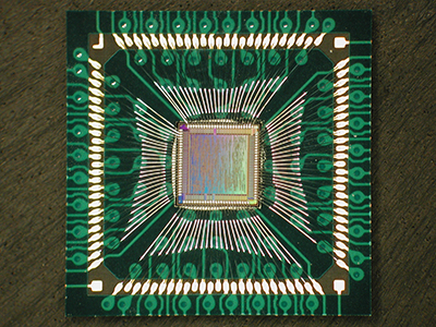
 Package & Product Development


 Intellectual Property


 Consulting


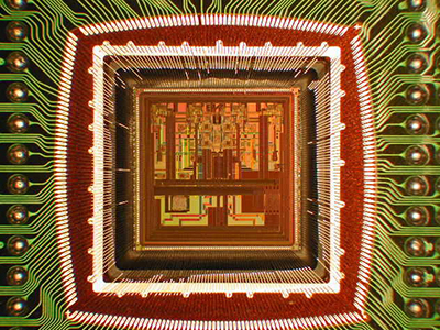
 Product Design & Development

 Product Design & Development
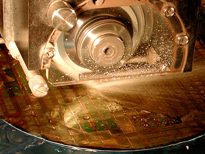
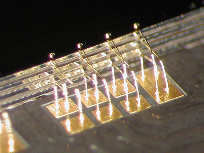
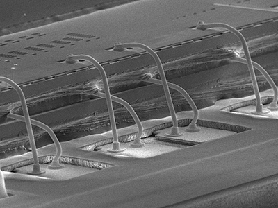
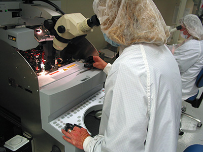
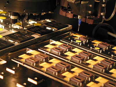
 Assembly & Fabrication Process


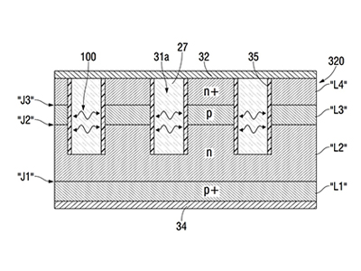
 Patent & IP Development


 Expert Witness Service

Product & Construction Analysis
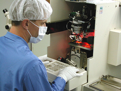
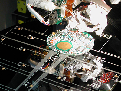
 Manfacturing Process & Systems
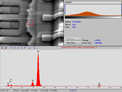
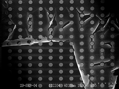
 Product & Construction Analysis